PLD

UHV Pulsed Laser Deposition System

Custom

Krypton fluoride (KrF) excimer, with a wavelength (λ)=248 nm.

The Pulsed Laser Deposition (PLD) is a thin film deposition in which a pulsed laser radiation shots a "target" sited on the beam focal plane, inside a vacuum chamber. The laser energy causes the ablation and the evaporation of the chemical compounds in the target and produces a flux of material, named "plume". Such a material, under form of plume, arrives on a substrate and, at the opportune growth conditions (substrate temperature, atmosphere pressure, etc.), the growth of a thin film takes place. Usually the plume (composed not only by ions and electrons, but also macromolecules or macroscopic particulates) conserves the stoichiometry of the target, equal to that composing the deposited film. Moreover, since the ablation of the target is assisted by the laser, the deposition can occur either in ultra high vacuum as well as in a background gas (up to several mbar). Ref: https://trieste.nffa.eu/areas/growth/pld/

ald-sm

Atomic Layer Deposition System

Savannah 100 ALD (Atomic Layer Deposition) from Cambridge NanoTech

The Savannah ALD (Atomic Layer Deposition) from Cambridge NanoTech is a low- to mid-temperature (100-250 ℃) deposition system that uses surface adsorbtion of single mono-layers of reactive precursor gases to form single atomic monolayers of a variety of insulating and conductive layers, with good uniformity, almost perfect conformality, and minimal heating of substrates. Deposition rates are typically rather slow, in the range of 3-6 Å per minute, but extremely high-aspect-ratio fill (20:1) is easily achievable. The process involves releasing alternating gas pulses of reactive metal-bearing organic precursors and oxidizing secondary precursors such as water, O2, or O3. Available deposition materials are Al2O3 (aluminum oxide) and HfO2 (hafnium oxide), TiO2 (titanium dioxide), ZnO (zinc oxide), all using water as the secondary precursor. ZrO and other materials are being explored. Ref: https://cns1.rc.fas.harvard.edu/tool/cambridge-nanotechultratech-savannah/

pvd 18

RF Magnetron Sputtering Deposition System

Kurt J. Lesker lab 18

The Kurt J Lesker (KJL) Lab 18 Sputtering System uses four shuttered magnetron guns containing 4” X .250” targets to sputter deposit single thin films or multiple stacked film layers on wafers up to 6” diameter, glass slides and small samples. Substrate heating and rotation is also available for enhanced film properties and improved film uniformity. This tool is equipped with one RF power supply for sputtering so only one material can be deposited at a time. Current materials approved for use in the KJL Lab 18 include (Si, SiO2, Si3N4, HfO2, TiO2, and ITO). In addition to the magnetron guns an ion source is also available for the etching of native oxide, deposited materials and for use during deposition to enhance uniformity. Process gases available on this system include Argon, Nitrogen, and Oxygen.

20180521_152948

Electron Beam Evaporation System

AJA International ATC Flagship Series Sputtering Systems

ATC-2400H   ATC SERIES EVAPORATION SYSTEM
TES-U            THERMAL EVAPORATION SOURCE
SHQ-4-U       UPGRADED SUBSTRATE HOLDER W/ HEATING CAPABILITIES


20180521_153018

Microwave Synthesis Reactor

Monowave 300 from Anton Paar

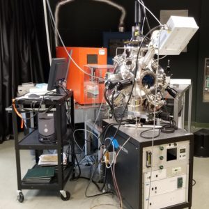
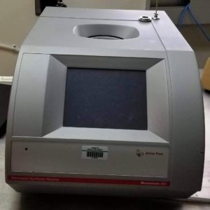
Monowave 300 reaches a new level in microwave assisted organic synthesis since it combines utmost user safety and facilitation of daily lab-work with the highest Anton Paar standards in terms of product quality, precise measurement and reaction control. Due to the prevention of temperature overshoots cleaner products (less by-products) can be obtained. With its operation limits of 300 °C and 30 bar, Monowave 300 opens up new reaction pathways for operation in R&D scale.

The extremely high field density guarantees outstanding heating rates in any scale and for any solvent. In addition to the standard borosilicate glass vials, a SiC vessel is available which provides ultra-fast heating even for microwave transparent reaction mixtures. Since SiC is chemically inert, fluorinations can also be performed without detaching the vessel material.

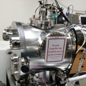
Monowave 300 accomodates 4 different reaction vials and volumes between 0.5 mL and 20 mL. The vials are sealed leak-proof with a PEEK snap cap and a PTFE-coated silicone septum - all consumables are completely reusable items. Due to the same neck sizes of the reaction vials, one and the same cap and septum can close any reaction vial just with the click of a thumb. In case of remaining post reaction overpressure the vials are automatically depressurized during the opening process of the cavity cover.

In addition to the IR sensor, the optional Ruby Thermometer can be used for accurate temperature monitoring. It is a fiber optic probe sensor for internal temperature control based on the temperature-dependent luminescence of a ruby crystal. With this simultaneous internal and IR temperature feedback reactions can be precisely controlled and monitored.

Rf: http://www.speciation.net/Database/Instruments/Anton-Paar-GmbH/Monowave-300-;i3043

Labstar500

Glove Box

LabStar Pro from MBraun
  • Compact design with integrated gas purifier unit
  • Modular box design for easy extension
  • Available in 12 sizes (single sided or double sided)
  • O2 and H2O < 1ppm
  • Closed loop circulation
  • Negative and positive pressure operation
unilabpro500

Glove Box

LabStar Pro from MBraun
  • Modular box design for easy extension
  • Available in 12 sizes (single sided or double sided)
  • Powerful gas purifier unit (DP as option for 24/7 purification)
  • O2 and H2O < 1ppm
  • Closed loop circulation
  • Negative and positive pressure operation
20180521_152224

Atomic Force Microscope

Dimension Icon ScanAsyst from Veeco
AFM Specifications
  • Minimum Feature Size Resolved, Z: ~0.1 nm
  • Minimum Feature Size Resolved, X & Y: ~2 nm
  • X & Y scan range: 90 μm x 90 μm
  • Z scan range: up to 10 μm
  • Z noise floor: <30 pm RMS in appropriate environment (imaging bandwidth up to 625 Hz)
  • Z sensor noise level(closed-loop): 35 pm RMS (imaging bandwidth up to 625 Hz); 50 pm RMS force curve bandwidth (0.1 Hz to 5 kHz)
  • X & Y position noise (closed-loop): ≤0.15 nm RMS (imaging bandwidth up to 625 Hz)
  • X & Y position noise (open-loop): ≤0.10 nm RMS (imaging bandwidth up to 625 Hz)
  • Integral nonlinearity (X-Y-Z): <0.5%
  • Sample Size: ≤210 mm diameter, ≤15 mm thick
  • Motorized position stage (X-Y axis): 180 mm × 150 mm inspectable area; 2 μm repeatability, unidirectional; 3 μm repeatability, bidirectional
  • Microscope optics: 5-megapixel digital camera; 180 μm to 1465 μm viewing area; Digital zoom and motorized focus
TEM

Transmission Electron Microscope

Hitachi HT7800

An Evolutionary Era of 120kV Transmission Electron Microscopy (TEM) with the Hitachi HT7800: New Technologies, Digital Designs, Automation, Ionic Liquids, and More!

With sub-2 angstrom resolution and the highest contrast in its class, the HT7800 incorporates advanced technologies to yield an electron microscope capable of easy operation by new and experienced users alike, whereby providing dual imaging modes, higher efficiency, excellent imaging quality, increased ergonomics, and adaptability for future needs.

20180521_152519

Scanning Electron Microscope

SU8010 from Hitachi
  • High resolution of 3.0 nm
  • Point and click PC interface
  • Auto and manual focus
  • Stage control
  • Dual magnification
  • Multipoint measurement
  • Digital zoom
  • Sample exchange
  • Easily mouse operated
  • Image capture
  • Digital image capture – Polaroid camera available
  • Large chamber and stage
  • 5 axis automation
  • Click-center-of-zoom
  • Automatic low vacuum system
  • Switch between LV and HV with one click
  • Specimen can be held at LV without being subjected to damaging effects of HV
  • EDS-UTW detector
  • CL detector
  • SEI/BEI detectors
20180521_152336

Ultra-High Resolution (1.0nm) Scanning Electron Microscope FE-SEM

Hitachi HT7800

SU8010 has excellent performance as the entry level model in the SU8000 series. The combination of Semi-in-lens type objective lens and cold FE-gun with small energy spread delivers ultra high resolution imaging performance and fl exible SE-BSE signal mixing using Hitachi’s detector technology for absolute surface information, Z-number contrast and charge suppression.
Ultra high resolution imaging (Resolution 1.0nm/15kV)


Beam deceleration function as standard (Resolution 1.3nm/1kV)
Beam deceleration applies a negative voltage (Beam deceleration voltage : Vd) to the specimen to decelerate the primary electron just before the beam interacts with the specimen. By using beam deceleration, landing voltage can be reduced as low as 100V with low lens aberration. As a result, ultra high resolution imaging of sample surface characteristics can be obtained at ultra low landing voltage.


Secondary Electron Image Resolution:
1.0nm (Vacc 15kV, WD=4mm)
1.3nm (landing voltage 1kV, WD=1.5mm)


Landing voltage 0.1~30kV:
Magnification 60x~2,000,000x*2

Stage control:
3-axis motor drive

20180521_152200

Electron Beam Lithography (EBL)

Pioneer from Raith

Electron Beam Lithography main specifications:
• Filament type Schottky-TFE
• Laserstage travel range 50x50x25 mm
• Beam size (resolution) ≤ 2.5 nm (≤ 1.6 nm *)
• Minimum feature size ≤ 20 nm (guaranteed)
• Field stitching ≤ 50 (60)nm (m+2σ) ** (guaranteed)
• Overlay accuracy (alignment) ≤ 50 (60)nm (m+2σ) **
• Beam current drift ≤ 0.5% / 1 hour
• Writing speed 2.5 MHz (10MHz optional)

20180521_152739

Ram Spectrometer

LabRam HR Evolution from Horiba Scientific

High spatial and spectral resolutions
HORIBA Scientific’s optimized design results in the most sensitive instruments on the market, with high throughput diffraction limited spatial resolution. Spectrally, the high resolution spectrometer allows subtle sample information such as crystallinity, polymorphism, strain and other band analysis to be characterized with ease.

Cover your sample from UV to NIR
Compatibility with a wide range of laser wavelengths and the possibility of mounting up to three detectors enables the measurement wavelength range to be extended from 200nm to 2100nm. The optimized UV configuration offers the best solution for UV Raman analysis with wavelengths below 400nm. Such performance opens up other spectroscopic techniques such as UV Raman, resonance Raman and photoluminescence, allowing detailed sample characterization from many varied materials.

Ease of use and ergonomy
The fully automated intelligent design of the LabRAM HR Evolution ensures ultimate performance coupled with ease of use; and the LabSpec 6 software allows full benefit from the unrivalled performances of the LabRAM HR Evolution at the touch of a button.